Tanaka-Ohya-Nakane-Anh Laboratory
Research feilds
- Electronic engineering, electronic properties of various materials and device engineering.
- Synthesis and formation of new materials and structures that do not exist in nature, such as heterostructures, alloy crystals, hybrid structures, and nanostructures composed of different materials.
- Exploration and control of their optical, electronic, magnetic, and spin-related properties and device applications.
- Fusion of semiconductors and magnetism (or ferromagnetism) and their application to electronics.
- Pioneering research on functional materials and devices utilizing spin degrees of freedom and “spintronics”.
- Fabrication of quantum materials, control of quantum states including spin and spin-orbit interactions, application to quantum information devices, and pioneering quantum science and technology.
In our laboratory, we are conducting basic research on new electronic materials and devices, considering their future application to electronic, optical, and magnetic (spin) devices, as well as their hybrid devices. Specifically,
- Epitaxial growth of nanometer-scale ultrathin films, artificial structures and quantum heterostructures with quantum mechanical effects, using various materials such as semiconductors, metals, semimetals, ferromagnetic materials, superconductors, and topological materials.
- Design and fabrication of new materials, that do not exist in the natural world at the atomic level, to study the material science and physical properties of these new materials, and to fabricate prototypes of devices to provide guidelines for future electronics applications. In particular, we are focusing on the creation of new materials, in which electron spin and its order (magnetism) are prominent, and their application to semiconductor electronics, “spintronics”. Furthermore, we are carrying out a variety of research activities on the control of spin, spin-orbit interaction, other quantum states to develop quantum science and technology.
Current research subjects
(For detail, see our recent publication list)
- Ferromagnetic/Semiconductor Hybrid Structures
- New III-V-based magnetic semiconductors and their quantum heterostructures
- Delta doping of magnetic elements in semiconductors and their heterostructures, ferromagnetic ordering at high temperatures
- Formation of semiconductor / ferromagnetic nanoparticle structures, exploration of physical properties, functional design, and device applications
- Spin-dependent transport, magneto-optic effects, and spin control in semiconductor heterostructures and their device applications
- Semiconductor-based epitaxial ferromagnetic tunnel junction devices
- New group-IV-based magnetic semiconductors, magnetic/semiconductor hybrid structures
- Spin transistors (Spin MOSFETs, Spin-Filter Transistors, etc. analysis and fabrication)
- Proposal and analysis of new reconfigurable logic circuits using spin transistors
- Process development and prototyping of spin devices
- Development and functional control of new topological-material / semiconductor heterostructures and quantum materials
- Formation of superconductor / ferromagnetic-semiconductor heterostructures and their application to electronic properties and quantum information devices
- Research based on the free ideas of students and researchers
Our laboratory conducts fundamental research on new electronic materials and devices with a view to future applications in electronic, optical, magnetic (spin), and quantum devices, as well as their hybrid devices. Specifically, we aim (1) to design and fabricate new materials, that do not exist in nature, by atomically controlled epitaxial growth of nanometer-scale ultrathin films, artificial nanostructures, and quantum heterostructures that exhibit quantum mechanical effects, using a variety of materials, including semiconductors, metals, semimetals, and ferromagnetic materials, superconductors and topological materials, and (2) to design and fabricate new materials at the atomic level to study the materials science and condensed matter physics of the new materials, and to fabricate prototypes of devices to provide guidelines for future electronics applications. In recent years, we have been especially focusing on pioneering research on “spintronics”, the creation of new materials, in which electron spin and its order (magnetism) are prominent, and their application to semiconductor electronics.
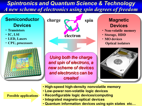
◆What is spin? You probably know that an electron is a negatively charged elementary particle. Since the invention of the transistor, the development of electronics and information technology (IT) in the latter half of the 20th century has been brought about mainly by various semiconductor devices that use the charge of the electron. On the other hand, electrons have another intrinsic property called “spin. Spin is a quantum mechanical concept, but in the language of classical mechanics, it corresponds to the rotation of the electron (spin angular momentum). Since this rotation never stops, we can say that the electron is itself a small electromagnet. In other words, by virtue of its “spin,” the electron is the world’s smallest permanent magnet. (As an aside, what is the world’s largest magnet? It is, of course, the earth.) The “spin” of electrons and the interaction between electrons make some materials ferromagnetic like permanent magnets (ferromagnets), and some materials exhibit superconductivity where the electrical resistance becomes zero.
◆Spintronics However, in semiconductors, which are used for electronics and information and communication technology, only the charge of electrons has been mainly used, and “spin”, another degree of freedom, has not been used. We believe that the “spin degree of freedom” must be actively used in semiconductor technology in the 21st century, and we are pioneering a new field called “spintronics”. This field is now a new research stream worldwide, partly due to our pioneering research contributions from about a quarter of a century ago. Research that pioneers the frontiers of science and technology requires a broad interest in electronics and information technology, as well as a deep understanding of and intellectual curiosity about basic sciences such as quantum mechanics and materials science.
― Examples of research themes(not limited to these)―
- Crystal growth by molecular beam epitaxy to create new (ferro)magnetic semiconductors, heterostructures, and nanostructures that exhibit ferromagnetism and spin-dependent properties
- Investigation, elucidation and control of optical, electronic, and spin properties exhibited by ferromagnetic semiconductors and their heterostructures
- Their application to optical, electronic, and spin devices
- Fabrication of semiconductor magneto-optic crystals and enhancement of magneto-optic effects using light localization and its application to optical devices
- Physics of tunnel magnetoresistance (TMR) effect and spin-dependent tunneling in semiconductor heterostructures
- Formation of semiconductor-ferromagnetic composite nanostructures and spin-dependent transport phenomena and their device applications
- Crystal growth and properties of epitaxial ferromagnetic metal/semiconductor heterostructures and their device applications
- Basic research on nonvolatile memory (MRAM) focusing on electronic conduction phenomena such as spin valve effect and tunneling magnetoresistance effect
- Spin device microfabrication process and device prototyping
- Proposal and analysis of spin transistors and spin MOSFETs utilizing spin degrees of freedom in semiconductor devices
- Research on operating principles and device physics of spin transistors and spin MOSFETs
- Research on quantum materials and devices for quantum computing and development of new physical properties such as quantum anomalous Hall effect, Majorana bound states, topological quantum states, and spin-triplet superconductivity
◆ Fe Based Ferromagnetic Semiconductors and Devices Applications
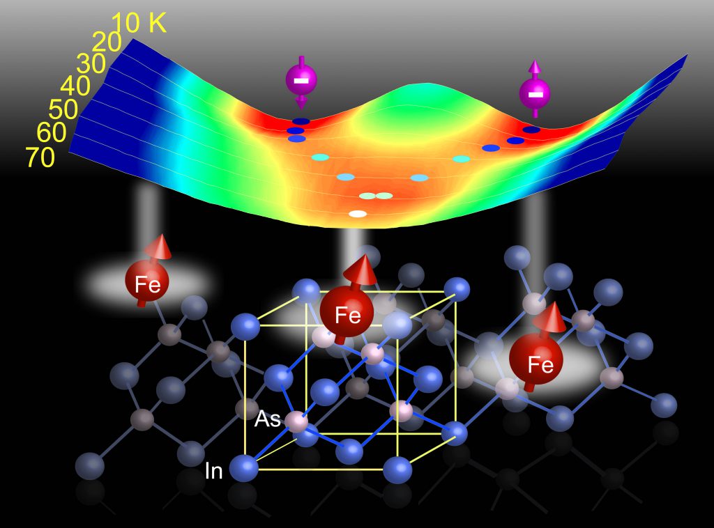
Ferromagnetic semiconductors (FMSs) with high Curie temperature (Tc) are highly desired for spintronic applications. So far, the mainstream study of FMSs is the Mn-doped III-V FMSs, which, however, have only p-type and Tc much lower than 300K. To search for new high-performance FMSs, there have been world-wide efforts that were mainly concentrated on wide-gap materials. However, reliable and systematic results have not yet been presented.
In this research, we present an alternative approach by using Fe instead of Mn as the magnetic dopants in narrow-gap III-V semiconductors; InAs, GaSb, and InSb. In these Fe-based FMSs, because the Fe atoms are in the isoelectronic Fe3+ state, the carrier type (electrons or holes) can be controlled independently by co-doping with non-magnetic dopants. These carriers would reside in the conduction band (CB) or the valence band (VB) of the host semiconductors and thus move faster with higher coherency. Using low-temperature molecular beam epitaxy, we have successfully grown single-phase crystal of both p-type FMS [(Ga,Fe)Sb [2]] and n-type FMSs [(In,Fe)As [3], (In,Fe)Sb [4]]. TC increases monotonically with the Fe content; and there is a tendency that TC is higher in narrower-gap host semiconductors. Intrinsic room-temperature ferromagnetism has been observed in (Ga1-x,Fex)Sb with x > 23% [2] and (In1-x,Fex)Sb with x > 16% [4]. In n-type FMS (In,Fe)As, large spontaneous spin splitting in the CB was observed, which is the first in all FMSs [5]. These results raise new issues in the magnetism of semiconductors and indicate that the Fe-doped III-V FMSs are promising for high-performance spintronic devices.
Ref: [1] N. T. Tu et al., APL 108, 192401 (2016). [2] P. N. Hai, APL 101, 182403 (2012). [3] N. T. Tu et al., arXiv:1706.00735 (2017). [4] L. D. Anh et al., PRB 92, 161201(R) (2015). [5] L. D. Anh et al., Nat. Commun. 7, 13810 (2016).
◆ Oxide-based spintronics
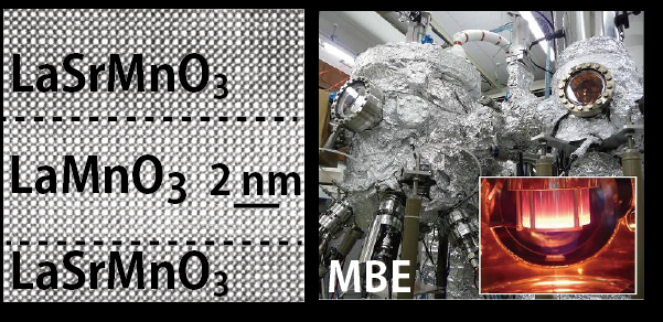
We are trying to explore new materials and physics for future oxide-based spintronics by developing various single-crystalline thin films, heterostructures, and magnetic nano structures.
More details on the ongoing projects can be found in the following homepage of prof. Ohya Research Group.
Message to prospective graduate students
Our laboratory is exploring new fields in materials science, devices, condensed matter physics, crystal engineering, and other areas of science and technology, and many of the themes we are studying are novel and challenging. Doctoral course students, as well as young students in master’s programs and graduation theses, can break into the forefront of research in a relatively short period of time, depending on their efforts, and we encourage them to do so (in fact, several students and young researchers have already made presentations at international conferences and are active at the forefront of academic conferences and community). Science-minded students can explore the scientific truth with intellectual curiosity, and engineering-minded students can try their hand at anything from device design to prototyping. We welcome students with a frontier spirit and full of ambition to enter and continue their studies. In order to conduct research in these new fields from a variety of approaches, we actively collaborate with excellent domestic and overseas research institutions, and have a record of joint research with research groups such as the National Institute of Advanced Industrial Science and Technology, the Department of Physics, Department of Applied Physics, Institute for Soli-State Physics at the University of Tokyo, and SPring-8.
Research is “discovering something unknown to the world, solving an unsolved problem for which no one knows the answer, or creating something (material, device, theory, concept, etc.) that no one has ever created before,” and is not something that can be done in a short period of time with a single hand. Research is a creative act, and results can only be achieved through wholehearted dedication. Research results require originality, speed, impact, and completeness. In the laboratory, students learn the value of creating something new, methodology, scientific and logical thinking, cooperation and collaboration with others, learning from failure, competing with the world, presenting and publishing research results, and responding to criticism and critique…etc., through working earnestly on specific research themes. Students will learn to think critically, cooperate and collaborate with others. Although it requires persistent and long-term efforts, the “something” that can only be achieved through diligent research on any subject brings a sense of fulfillment that only those who have experienced it can understand. This basic principle will not change even if you replace “research” with “business,” “management,” “creative work,” or “life. In your graduation thesis and graduate school, you will learn “the meaning of creativity” through serious efforts in “research,” and this is where you will gain nourishment for your long career and life afterwards.
We welcome laboratory tours and other visits.
- Contact: Professor Masaaki Tanaka
- Email: Masaaki[at]ee.t.u-tokyo.ac.jp
- (Please replace [at] with @ in the email.)
See also for the Department of Electrical Engineering, Graduate School of Engineering, The University of Tokyo and for the Department of Electronic Information Engineering and Electrical and Electronic Engineering. There is information about graduate school admissions, majors, and departments.